PCB Potting Compound: An In-Depth Analysis
PCB Potting Compound: An In-Depth Analysis
Printed Circuit Boards (PCBs) are critical components in modern electronics, serving as the foundation for virtually all electronic devices. PCB potting compounds play a crucial role in ensuring their longevity and reliability, especially in harsh environments. This comprehensive guide will explore PCB potting compounds’ purpose, types, benefits, and application processes, providing a detailed understanding of their importance in electronics.
1. Understanding PCB Potting Compounds
PCB potting compounds are specialized materials used to encase and protect printed circuit boards. The primary goal of potting is to shield PCBs from environmental factors such as moisture, dust, and mechanical stress, thereby enhancing their durability and reliability. Potting compounds are typically used to fill the voids and cavities of electronic assemblies, creating a protective barrier around sensitive components.
1.1. Purpose and Benefits
The primary purposes of PCB potting compounds include:
- Environmental Protection:Potting compounds protect PCBs from moisture, chemicals, and contaminants, preventing corrosion and degradation of electronic components.
- Mechanical Protection:Potting compounds absorb mechanical shocks and vibrations by providing a cushioning layer, reducing the risk of damage to delicate components.
- Electrical Insulation:Potting compounds offer electrical insulation, preventing short circuits and ensuring the safe operation of the PCB.
- Thermal Management:Some potting compounds have thermal conductivity properties that help dissipate heat generated by electronic components, improving overall performance and reliability.
1.2. Types of PCB Potting Compounds
Several types of potting compounds are available, each with specific properties suited for different applications:
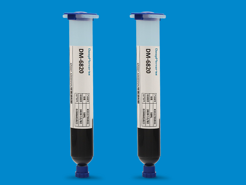
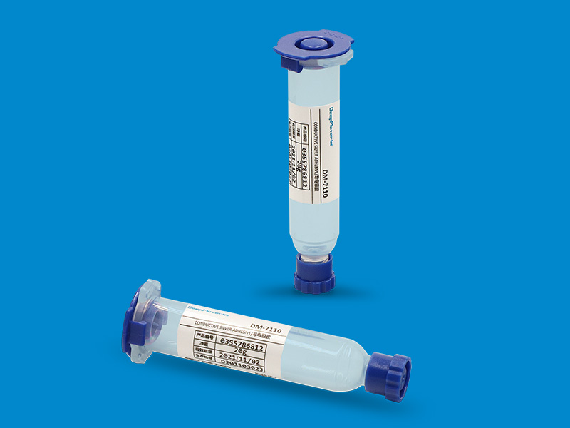
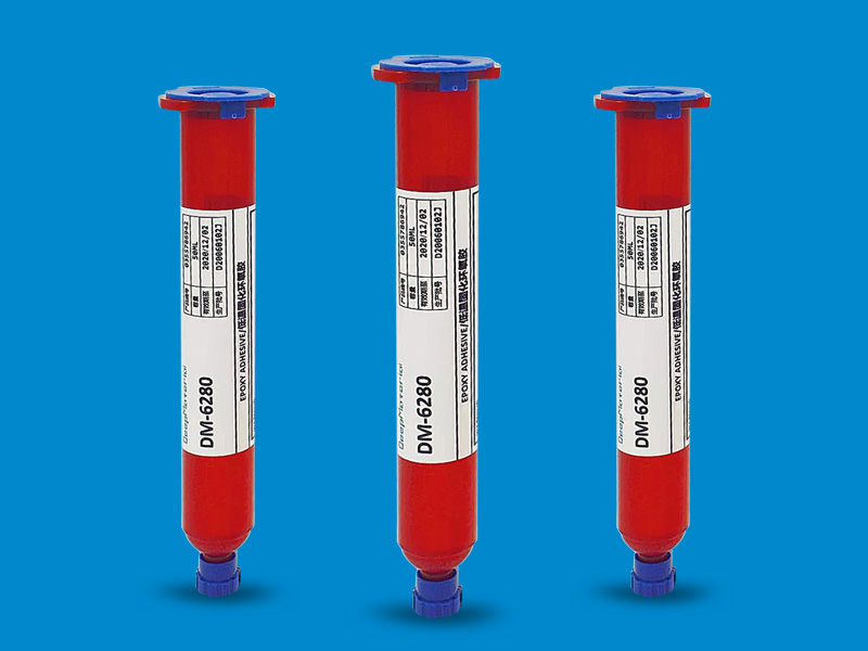
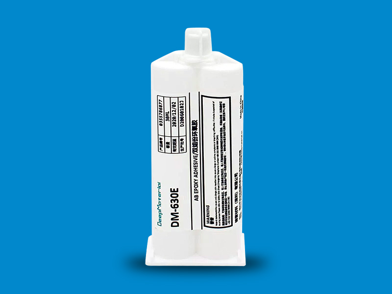
- Epoxy Resins:Epoxy resins are widely used in PCB potting due to their excellent adhesion, mechanical strength, and chemical resistance. They are suitable for environments with high humidity and harsh chemicals.
- Silicone Compounds:Silicone potting compounds offer superior flexibility and thermal stability. They are ideal for applications requiring resistance to extreme temperatures and vibrations.
- Polyurethane Compounds:Polyurethane potting compounds provide a good balance of flexibility and chemical resistance. They are commonly used in automotive and aerospace applications.
- Acrylic Resins:Acrylic potting compounds are known for their fast curing times and ease of application. They are often used in consumer electronics and low-cost applications.
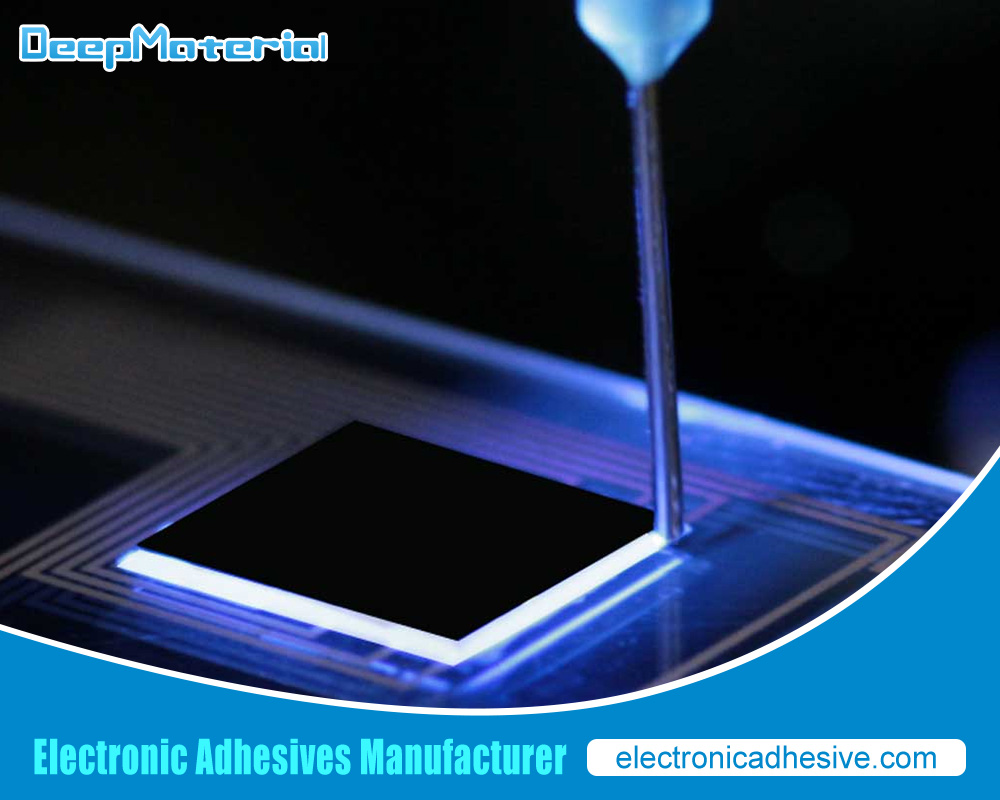
2. Application Process of PCB Potting Compounds
Applying PCB potting compounds involves several vital steps to ensure optimal performance and protection.
2.1. Preparation
Before applying potting compounds, it is essential to prepare the PCB correctly. This includes:
- Cleaning:Thoroughly clean the PCB to remove contaminants such as dust, grease, or residues. This step is crucial for ensuring proper adhesion of the potting compound.
- Drying:Ensure the PCB is completely dry before application. Moisture on the surface can interfere with the curing process and compromise the effectiveness of the potting compound.
2.2. Application Methods
Different application methods are used depending on the type of potting compound and the specific requirements of the PCB:
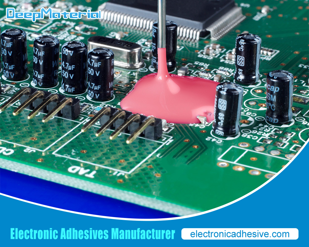
- Manual Pouring:Manual pouring is a standard method for small-scale applications or prototypes. The potting compound is poured directly onto the PCB and allowed to flow into all cavities.
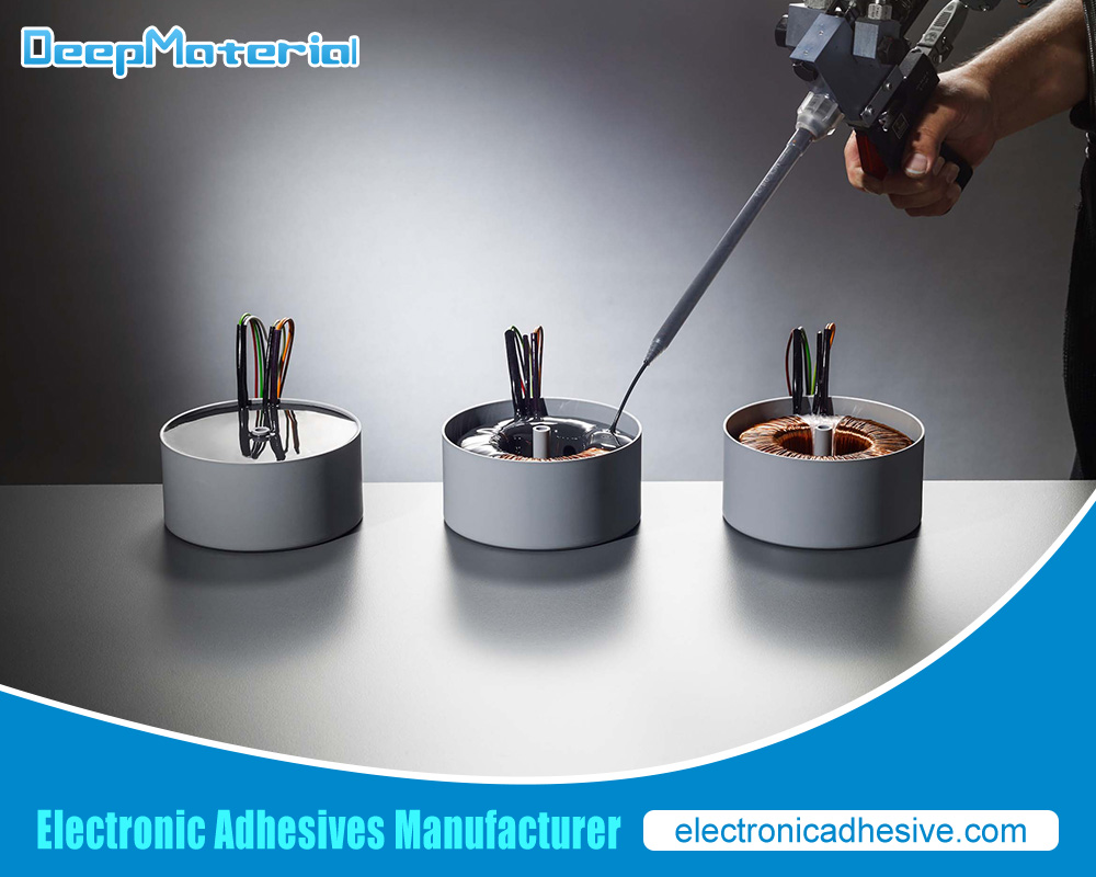
- In high-volume production, injection molding is used to apply the potting compound precisely. The compound is injected under pressure into a PCB mold, ensuring uniform coverage.
- Vacuum Deaeration:Vacuum Deaeration may remove air bubbles and ensure the complete filling of voids. The potting compound is placed in a vacuum chamber to eliminate trapped air before application.
2.3. Curing
After application, the potting compound must cure to achieve its final properties. Curing can be achieved through:
- Heat Curing:Some potting compounds require heat to cure. To facilitate curing, the PCB is placed in an oven or heat chamber.
- Room Temperature Curing:Certain compounds cure at room temperature, eliminating the need for additional heating equipment. This method is commonly used for epoxy and acrylic resins.
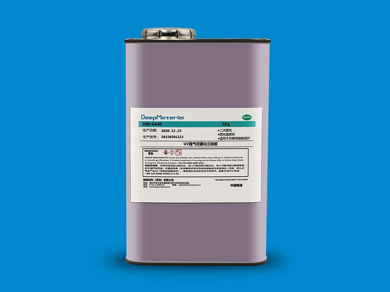
- UV Curing:UV-curable potting compounds require exposure to ultraviolet light to initiate curing. This method provides rapid curing and is suitable for applications where speed is essential.
3. Challenges and Considerations
While PCB potting compounds offer numerous benefits, there are also challenges and considerations to keep in mind:
3.1. Compatibility
Selecting a suitable potting compound is crucial for compatibility with the PCB materials and components. Incompatible compounds can lead to issues such as chemical reactions, poor adhesion, or degradation of sensitive components.
3.2. Environmental Factors
Different potting compounds have varying levels of resistance to environmental factors. It is essential to choose a compound that matches the specific ecological conditions the PCB will be exposed to, such as temperature extremes, humidity, and chemical exposure.
3.3. Application Precision
Achieving consistent and precise application of the potting compound is essential for adequate protection. Inaccurate application can lead to incomplete coverage, air bubbles, or uneven curing, compromising the PCB’s performance.
3.4. Cost Considerations
The cost of potting compounds can vary based on the type and performance characteristics. It is important to balance cost with the required level of protection and performance to ensure cost-effective solutions.
4. Future Trends and Innovations
The field of PCB potting compounds is continuously evolving, with ongoing research and development aimed at improving performance and addressing emerging challenges. Some notable trends and innovations include:
4.1. Advanced Materials
Researchers are exploring new materials with enhanced properties, such as improved thermal conductivity, flexibility, and chemical resistance. Advanced materials aim to meet the growing demands of modern electronics, including miniaturization and high-performance applications.
4.2. Eco-Friendly Solutions
With increasing environmental awareness, there is a push for eco-friendly potting compounds that reduce ecological impact. Biodegradable and low-VOC (volatile organic compound) options are being developed to address sustainability concerns.
4.3. Smart Potting Compounds
Innovative potting compounds with embedded sensors and monitoring capabilities are being explored. These smart compounds can provide real-time feedback on the PCB’s condition, detecting issues such as temperature fluctuations or mechanical stress.
4.4. Enhanced Application Techniques
Advancements in application techniques, such as automated dispensing and precision curing methods, are improving the efficiency and consistency of potting processes. These techniques aim to reduce production costs and enhance the overall quality of the final product.
Conclusion
PCB potting compounds are essential for protecting and enhancing the performance of printed circuit boards in various electronic applications. By providing environmental protection, mechanical cushioning, and electrical insulation, potting compounds ensure the reliability and longevity of electronic devices. Understanding the types, application processes, and challenges associated with potting compounds is crucial for selecting the right solution for specific needs. As technology advances, ongoing research and innovation continue to drive improvements in potting materials and techniques, shaping the future of electronic protection.
With this comprehensive understanding of PCB potting compounds, you can make informed decisions about their application and benefits, ensuring your electronic devices’ optimal performance and durability.
For more about choosing the Top PCB Potting Compound: An In-Depth Analysis, you can pay a visit to DeepMaterial at https://www.electronicadhesive.com/ for more info.